- 您现在的位置:买卖IC网 > Sheet目录505 > RXM-GPS-SG-T (Linx Technologies Inc)GPS MODULE SMD SIRF
�� �
�
�BOARD� LAYOUT� GUIDELINES�
�The� module’s� design� makes� integration� straightforward;� however,� it� is� still� critical�
�to� exercise� care� in� PCB� layout.� Failure� to� observe� good� layout� techniques� can�
�result� in� a� significant� degradation� of� the� module’s� performance.� A� primary� layout�
�goal� is� to� maintain� a� characteristic� 50-ohm� impedance� throughout� the� path� from�
�the� antenna� to� the� module.� Grounding,� filtering,� decoupling,� routing� and� PCB�
�stack-up� are� also� important� considerations� for� any� RF� design.� The� following�
�section� provides� some� basic� design� guidelines� which� may� be� helpful.�
�During� prototyping,� the� module� should� be� soldered� to� a� properly� laid-out� circuit�
�board.� The� use� of� prototyping� or� “perf”� boards� will� result� in� poor� performance� and�
�is� strongly� discouraged.�
�The� module� should,� as� much� as� reasonably� possible,� be� isolated� from� other�
�components� on� your� PCB,� especially� high-frequency� circuitry� such� as� crystal�
�oscillators,� switching� power� supplies,� and� high-speed� bus� lines.�
�When� possible,� separate� RF� and� digital� circuits� into� different� PCB� regions.� Make�
�sure� internal� wiring� is� routed� away� from� the� module� and� antenna,� and� is� secured�
�to� prevent� displacement.�
�Do� not� route� PCB� traces� directly� under� the� module.� There� should� not� be� any�
�copper� or� traces� under� the� module� on� the� same� layer� as� the� module,� just� bare�
�PCB.� The� underside� of� the� module� has� traces� and� vias� that� could� short� or� couple�
�to� traces� on� the� product’s� circuit� board.�
�The� Pad� Layout� section� shows� a� typical� PCB� footprint� for� the� module.� A� ground�
�plane� (as� large� and� uninterrupted� as� possible)� should� be� placed� on� a� lower� layer�
�of� your� PC� board� opposite� the� module.� This� plane� is� essential� for� creating� a� low�
�impedance� return� for� ground� and� consistent� stripline� performance.�
�Use� care� in� routing� the� RF� trace� between� the� module� and� the� antenna� or�
�connector.� Keep� the� trace� as� short� as� possible.� Do� not� pass� under� the� module�
�or� any� other� component.� Do� not� route� the� antenna� trace� on� multiple� PCB� layers�
�as� vias� will� add� inductance.� Vias� are� acceptable� for� tying� together� ground� layers�
�and� component� grounds� and� should� be� used� in� multiples.�
�Each� of� the� module’s� ground� pins� should� have� short� traces� tying� immediately� to�
�the� ground� plane� through� a� via.�
�Bypass� caps� should� be� low� ESR� ceramic� types� and� located� directly� adjacent� to�
�the� pin� they� are� serving.�
�A� 50-ohm� coax� should� be� used� for� connection� to� an� external� antenna.� A� 50-ohm�
�transmission� line,� such� as� a� microstrip,� stripline� or� coplanar� waveguide� should�
�be� used� for� routing� RF� on� the� PCB.� The� Microstrip� Details� section� provides�
�additional� information.�
�In� some� instances,� a� designer� may� wish� to� encapsulate� or� “pot”� the� product.�
�There� is� a� wide� variety� of� potting� compounds� with� varying� dielectric� properties.�
�Since� such� compounds� can� considerably� impact� RF� performance� and� the� ability�
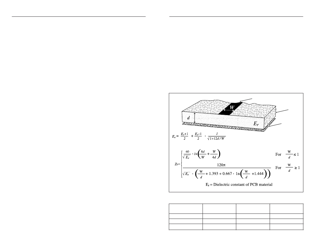
�MICROSTRIP� DETAILS�
�A� transmission� line� is� a� medium� whereby� RF� energy� is� transferred� from� one�
�place� to� another� with� minimal� loss.� Common� forms� of� transmission� lines� are� coax�
�cable,� microstrip,� stripline,� and� coplanar� waveguides.� Since� a� microstrip� is�
�straightforward� to� understand� we� will� focus� on� it� here.� Other� forms� of�
�transmission� lines� may� also� be� utilized.�
�The� term� “microstrip”� refers� to� a� PCB� trace� running� over� a� ground� plane� that� is�
�designed� to� serve� as� a� transmission� line.� The� width� of� the� trace� is� based� on� the�
�desired� characteristic� impedance� of� the� line� (in� this� case� 50� ohms),� the�
�thickness� of� the� PCB,� and� the� dielectric� constant� of� the� board� material.� For�
�standard� 0.062in� thick� FR-4� board� material,� the� trace� width� would� be� 111� mils.�
�The� correct� trace� width� can� be� calculated� for� other� widths� and� materials� using�
�the� information� below.� Handy� software� for� calculating� microstrip� lines� is� also�
�available� on� the� Linx� website,� www.linxtechnologies.com.� There� is� also� a� variety�
�of� free� programs� and� design� tools� available� from� other� sources� which� can� be�
�found� readily� on� the� internet.�
�Trace�
�Board�
�Ground� plane�
�Figure� 8� :� Microstrip� Formulas�
�to� rework� or� service� the� product,� it� is� the� responsibility� of� the� designer� to� evaluate�
�and� qualify� the� impact� and� suitability� of� such� materials.�
�Dielectric� Constant� Width/Height� (W/d)�
�Effective� Dielectric�
�Constant�
�Characteristic�
�Impedance�
�Page� 2� 8�
�4.� 8� 0�
�4.00�
�2.55�
�1.� 8�
�2.0�
�3� .0�
�3� .59�
�3� .07�
�2.12�
�50.0�
�51.0�
�4� 8� .0�
�Page� 29�
�发布紧急采购,3分钟左右您将得到回复。
相关PDF资料
RXM-GPS-SR-T
GPS MODULE SMD SIRF W/ANT
RZE002P02TL
MOSFET P-CH 20V 200MA EMT3
RZF020P01TL
MOSFET P-CH 12V 2A TUMT3
RZF030P01TL
MOSFET P-CH 12V 3A TUMT3
RZM002P02T2L
MOSFET P-CH 20V 0.2A UMT6
RZQ045P01TR
MOSFET P-CH 12V 4.5A TSMT6
RZQ050P01TR
MOSFET P-CH 12V 5A TSMT6
RZR020P01TL
MOSFET P-CH 12V 2A TSMT3
相关代理商/技术参数
RXM-GPS-SR-B
功能描述:GPS模块 GPS Receiver with Integrated Antenna
RoHS:否 制造商:Linx Technologies 频带:1.575 GHz 通道数量:20 首次定位时间(冷启动):35 s 获取敏感性:- 144 dBm 水平位置精确度:10 m 工作电源电压:3 V to 4.2 V 工作电源电流:46 mA 接口类型:Serial 最大工作温度:+ 85 C 安装风格:SMD/SMT 尺寸:15 mm x 13 mm x 2.2 mm
RXM-GPS-SR-T
功能描述:GPS模块 GPS Receiver with Integrated Antenna
RoHS:否 制造商:Linx Technologies 频带:1.575 GHz 通道数量:20 首次定位时间(冷启动):35 s 获取敏感性:- 144 dBm 水平位置精确度:10 m 工作电源电压:3 V to 4.2 V 工作电源电流:46 mA 接口类型:Serial 最大工作温度:+ 85 C 安装风格:SMD/SMT 尺寸:15 mm x 13 mm x 2.2 mm
RXM-UHF
制造商:RADIOMETRIX 制造商全称:RADIOMETRIX 功能描述:UHF Radio Telemetry Receiver Module
RXP0005
制造商:Panasonic Industrial Company 功能描述:ARM
RXP0014
制造商:Panasonic Industrial Company 功能描述:PULLEY
RXP0015
制造商:Panasonic Industrial Company 功能描述:ROLLER
RXP0016
制造商:Panasonic Industrial Company 功能描述:ROLLER
RXP0016-4
制造商:Panasonic Industrial Company 功能描述:ROLLER